The surface of a material is where it interacts with the world. In semiconductors, thin films, batteries, coatings, catalysts and advanced functional materials, the first few nanometres define adhesion, electrical behaviour, corrosion resistance, contamination risk, diffusion pathways and long-term reliability.
Secondary Ion Mass Spectrometry, or SIMS, is among the most sensitive surface analysis techniques available. Because it is based on mass spectrometry, it can provide isotopic as well as elemental information, together with some molecular information. SIMS can analyse material to depths of a few microns, while maintaining a depth resolution of a few nanometres.
We sat down with Dr. Graham Cooke, Principal Scientist at Hiden Analytical, to discuss why SIMS is so important in modern materials science, how Hiden’s SIMS and SNMS instrumentation supports advanced research, and what researchers should consider when choosing a surface analysis platform.
Graham, for readers working in advanced materials, why is SIMS such a critical surface analysis technique?
SIMS originally emerged from the semiconductor industry, where it was developed to detect very small quantities of dopant elements in high-purity silicon and gallium arsenide crystals, often at parts-per-million and parts-per-billion levels.
Over time, the advantages of high sensitivity, excellent depth resolution and the ability to produce composition maps have led to its use across many industries. SIMS is now applied to the analysis of thin layers, particles, contaminants, isotopic enrichment and trace species.
SIMS is critical for sectors such as semiconductors, photovoltaics, batteries, optical coatings, polymers, nuclear materials and advanced thin films, where functional performance is often governed by chemistry at interfaces and near surfaces.
Can you explain the fundamental principles of SIMS and how it enables high-sensitivity analysis?
SIMS is a mass spectrometry technique. Mass spectrometers detect atoms and molecules by separating and identifying them according to their mass. Conventional mass spectrometry generally ionises gas samples, but SIMS works with solids.
To achieve this, a finely focused beam of ions, known as the primary ion beam, is directed at the sample surface under vacuum. On impact, material is ejected from the upper layers of the sample in a process known as sputtering. A fraction of this sputtered material is ionised and can then be extracted by an electric field into the mass spectrometer and analysed.
Most of the sputtered material is neutral, but a small fraction is ionised. These secondary ions are extracted and analysed by the mass spectrometer to identify the elemental, isotopic or molecular species present.
The important point is that SIMS is inherently surface-sensitive. We are not averaging through a large bulk volume; we are interrogating the outermost layers of atoms.
A major advantage is that the ion beam can be rastered across the surface to build a chemical map. As material is removed, deeper layers are exposed, allowing a chemical depth profile to be generated. By stacking these images, a full 3D chemical map can be built, showing how selected species vary through a thin film, coating, interface or implanted region.
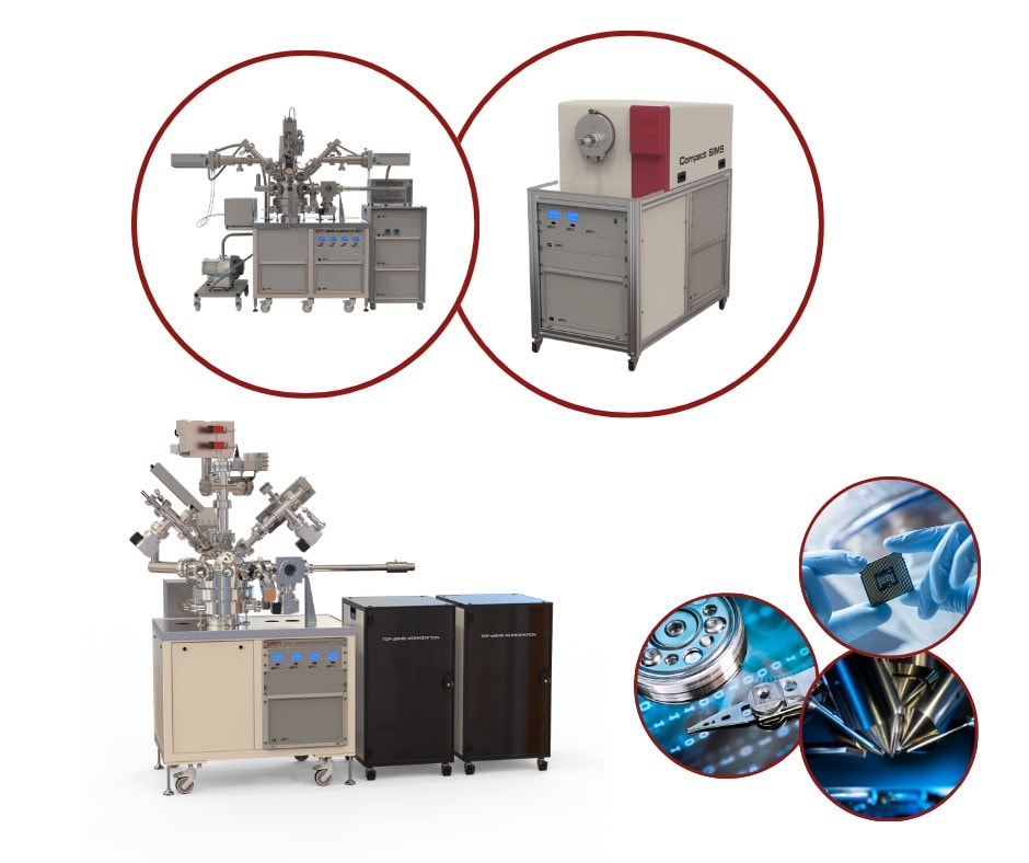
Hiden’s SIMS Workstation is designed for both dynamic and static SIMS, allowing detailed composition analysis and depth profiling in a single instrument platform.
You mentioned static and dynamic SIMS. How do these modes differ analytically, and how does that influence the type of information obtained by the researcher?
The terms static and dynamic SIMS relate to the amount of material removed during analysis.
When the ion dose is very low, the surface is not appreciably eroded. In static SIMS, perhaps only around 1% of the surface atoms are affected. Because the surface remains effectively intact, static SIMS is valuable for highly surface-specific analysis, particularly where molecular fragments, organic species, residues or very shallow contamination are important.
As the ion dose is increased, the surface is removed and the underlying layers are exposed for analysis. This is dynamic SIMS, which is generally used for depth profiling. In this mode, material is deliberately removed in a controlled way so that changes in composition can be monitored as a function of depth. This is particularly valuable for dopant profiling, diffusion studies, multilayer coatings, implanted materials and thin film stacks.
Dynamic SIMS can also be quantitative when suitable standards, calibration methods and matrix corrections are used.
The advantage of Hiden’s SIMS Workstation is that it can perform both static and dynamic SIMS analysis in a consolidated system. It also supports positive and negative secondary ion detection and can be configured with mass range options up to 5000 amu.
What kinds of materials challenges is SIMS well suited to tackling?
SIMS is very good at answering questions such as: what contaminants are present at the surface, how far have they penetrated, whether a dopant has reached the required depth, whether a multilayer structure has been deposited correctly, or whether an interface is chemically abrupt or diffuse.
For example, in semiconductor and electronic materials, SIMS can help evaluate dopant distributions, trace impurities and diffusion across device layers. In thin film and coating research, it can reveal how elements vary through optical coatings, protective layers or functional films. In battery materials, SIMS can help explore ion transport, degradation products and interfacial chemistry. In polymers and surface-treated materials, it can detect residues, additives, surface modifications and contamination.
That combination of high sensitivity, depth profiling and chemical specificity is why SIMS remains so valuable for advanced materials R&D and failure analysis.
Where does Hiden Analytical’s instrumentation sit within the surface analysis workflow?
Hiden’s SIMS instruments can be configured and built around a customer’s specific requirements. This means users are not paying for features or complexity they do not need. It also means that, especially with the SIMS Workstation, systems can be reconfigured or upgraded in the future.
There are three major platforms: the Compact SIMS, AutoSIMS and SIMS Workstation. The first two are designed as almost “plug and play” instruments. They are ideal for routine analysis in industry and research and can be run from simple recipes. Their ease of use also makes them suitable for teaching.
The SIMS Workstation can be equipped with multiple ion guns, detectors and a high-precision stage, making it a very flexible but easy-to-use instrument. After spending more than five years running SIMS for contract analysis, I learned what works well, and what works less well, from a user’s perspective. The SIMS Workstation was developed from those lessons. It is a reliable, easy-to-operate tool, ideal for routine and general measurements, but it also offers a full range of research features that experienced users can explore.
We should also remember that Hiden produces SIMS systems that can be fitted to other instrumentation. The ultimate example is the Modular SIMS, often described as SIMS-on-a-Flange, where an ion gun, SIMS detector, electron gun and camera are mounted on a single DN200 flange. This has applications ranging from nuclear research to ensuring wafer cleanliness in semiconductor MBE.
Can you talk more about the Hiden SIMS Workstation and the technical capabilities it offers for depth profiling and compositional analysis?
The SIMS Workstation is the flagship platform for high-performance SIMS analysis. It provides a comprehensive solution for compositional analysis and depth profiling across surface analysis, thin film engineering, nanotechnology, fuel cell research and related areas. It is highly customisable, which is important because SIMS users rarely have identical requirements.
The Workstation can support dual-polarity ion collection, allowing both positive and negative secondary ions to be detected. It also provides high-sensitivity detection, depth profiling with imaging, and 3D data reconstruction. Automatic SIMS ion optics lens tuning and automatic mass alignment help improve usability and consistency.
This matters because SIMS can be a demanding technique. The instrumentation has to provide sensitivity, vacuum performance, ion beam control, sample handling and data acquisition in a way that supports both research flexibility and reliable day-to-day operation.
How does SNMS complement SIMS?
SNMS, or Sputtered Neutral Mass Spectrometry, complements SIMS by analysing sputtered neutral species rather than only the ionised fraction emitted directly from the surface. In practice, this can be very useful when researchers want more quantitative information, especially for higher-concentration species, alloys, oxides and coatings.
SIMS is exceptionally sensitive, but secondary ion yields can vary strongly with matrix chemistry. SNMS addresses this by focusing on sputtered neutrals, which can provide a more representative view of material composition in certain applications.
Hiden combines SNMS capability into its SIMS Workstation platforms. The SIMS Workstation includes an integrated ioniser for efficient SNMS analysis, which is useful for quantification of high-concentration elements, such as those found in alloys.
How does the Compact SIMS system support laboratories that need near-surface analysis in a more accessible platform?
The Compact SIMS is designed for users who need sensitive SIMS capability in a smaller, more accessible platform. It is aimed at fast and straightforward characterisation of layer structures, surface contamination and impurities, with an oxygen primary ion beam for sensitive positive ion detection and isotopic sensitivity across the periodic table. The ion gun geometry is optimised for nanometre-scale depth resolution and near-surface analysis.
One of the practical advantages is usability. The Compact SIMS has a small footprint, a rotary carousel that allows 10 samples to be loaded, and the same control software and ion gun system as the fully featured SIMS Workstation family. It can provide depth profiles, 2D and 3D images, and mass spectral data.
That makes it particularly attractive for laboratories that want powerful near-surface analysis capability but may not require the full level of customisation offered by a larger UHV workstation. The instrument is semi-portable and requires only mains power and a gas bottle to operate.
Hiden also offers ToF-qSIMS. What additional analytical capability does this bring, particularly in terms of molecular information, imaging and depth profiling?
ToF-qSIMS is interesting because it combines the strengths of quadrupole SIMS with time-of-flight SIMS in one system — a real best-of-both-worlds approach.
The SIMS Workstation is an excellent inorganic analysis tool with great sensitivity for elements. Adding the ToF spectrometer allows the detection of larger molecular fragments, such as those from polymers and pharmaceutical products. It also improves static SIMS capability for surface contamination studies.
The time-of-flight capability adds parallel data collection and molecular fragment analysis, while the quadrupole SIMS capability provides high-dynamic-range depth profiling. That is especially powerful when both spatially resolved chemical information and robust depth profiling are required.
ToF-qSIMS also supports hyperspectral imaging, 2D and 3D mapping, full spectral analysis pixel by pixel, and high-sensitivity SNMS mode for quantitative analysis of metallurgical thin films, oxides, alloys and coatings.
How important is imaging in modern SIMS?
It is becoming increasingly important. Researchers often do not just want a single depth profile; they want to understand lateral distribution as well. Is the contaminant localised? Is the dopant uniform? Is there segregation at grain boundaries? Is a defect chemically different from the surrounding material?
SIMS imaging provides high-resolution surface chemical mapping, while SIMS Mapper software supports 3D imaging, flexible depth profile gating, live image and depth profile windows, and data export for further processing.
This imaging capability changes the way researchers interpret materials. Instead of treating a sample as a single average composition, they can start to see spatial chemistry: where species are located, how they overlap, and how chemistry evolves through the depth of a structure.
It is also worth remembering that, in some cases, a picture is worth a thousand words. A 3D image is often easier for a report reader to understand than a quantified depth profile alone.
Across which application areas do you see SIMS delivering the greatest value for advanced materials research and process development?
There are several.
In semiconductors and electronic materials, SIMS is highly valuable for dopant profiling, contamination control, diffusion studies and thin film process development.
In photovoltaics and flexible solar cells, it can help evaluate multilayer structures and trace species that influence performance. Dual-polarity detection is especially valuable here, as you may only get one opportunity to analyse a contamination particle.
In battery research, the isotopic sensitivity of SIMS can support studies of ion migration, layer degradation and interfacial chemistry. SIMS is exceptionally sensitive to lithium, an element that many other techniques struggle to analyse.
In coatings and thin films, SIMS provides insight into layer uniformity, intermixing, adhesion-related chemistry and contamination.
It is also relevant in polymers, pharmaceuticals, corrosion studies, nuclear materials, superconductors, ceramics and advanced alloys. The common theme is that surface or interface chemistry strongly affects performance, and SIMS gives researchers a way to explore that chemistry with high sensitivity and spatial resolution.
Hiden’s surface analysis instrument range includes the SIMS Workstation, ToF-qSIMS Workstation, Compact SIMS, AutoSIMS, FIB-SIMS, Modular SIMS, EQS, MAXIM and associated ion sources, allowing users to select or configure systems around their specific application requirements.
What technical considerations should researchers take into account when selecting a SIMS system for their application?
From my time undertaking contract analysis, I think the primary consideration is understanding exactly what needs to be measured. What question do you want to answer?
Once that is known, it is usually straightforward to determine the correct instrument and analytical method. We are always on hand to assist customers with method development and data interpretation. That is where Hiden’s application knowledge becomes valuable.
The instrument is only part of the answer. The configuration, ion source selection, sample handling, software workflow and analytical method all need to be aligned with the application.
Finally, what message would you give to researchers looking to strengthen their surface analysis capability?
I would say that surface analysis should be considered early, not as an afterthought. Many development problems in advanced materials come down to surfaces and interfaces: contamination, diffusion, poor adhesion, unexpected oxidation, process residues, dopant movement or layer non-uniformity. SIMS gives researchers a direct way to investigate these issues with sensitivity and depth resolution that are difficult to achieve by other methods.
We can support that work with configurable SIMS and SNMS instruments, from Compact SIMS through to high-performance SIMS Workstations and ToF-qSIMS systems. Whether the goal is fundamental research, process optimisation, failure analysis or routine materials characterisation, the aim is the same: to give researchers chemically meaningful information from the region of the material where performance is often decided.
Graham Cooke Biography
Dr. Graham Cooke is Principal Scientist at Hiden Analytical. He was awarded a PhD in Physics by the University of Warwick in 1992 for research into semiconductor dopant profiling, sponsored by Plessey Research. He subsequently remained at Warwick, where he designed, built and used SIMS instrumentation for advanced materials analysis. In 2000, he became part-owner of a contract analysis laboratory specialising in complex materials characterisation, with a particular focus on semiconductor applications. Graham joined Hiden Analytical in 2006 as a system design specialist, working on custom large-scale instrumentation and SIMS systems. Today, he leads Hiden’s SIMS technology development while also contributing to the company’s broader mass spectrometry product portfolio.